


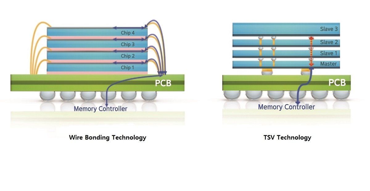
The thickness of the package (720?) remains the same as current 8-layer High Bandwidth Memory-2 (HBM2) products, which is a tremendous advancement in component design. This will help customers release next-generation, high-capacity products with better performance capacity without having to change their system configuration designs. Additionally, the 3D packaging technology also features a shorter data transmission time between chips than the currently existing wire bonding technology, resulting in considerably faster speed and lower power consumption.
“Packaging technology that secures all of the intricacies of ultra-performance memory is becoming tremendously important, with the wide variety of new-age applications, such as artificial intelligence (AI) and High Power Computing (HPC),” said Hong-Joo Baek, executive vice president of TSP (Test & System Package) at Samsung Electronics.
“As Moore’s law scaling reaches its limit, the role of 3D-TSV technology is expected to become even more critical. We want to be at the forefront of this state-of-the-art chip packaging technology.”
Relying on its 12-layer 3D-TSV technology, Samsung will offer the ultimate DRAM performance for applications that are data-intensive and amazingly high-speed. Also, by enhancing the number of stacked layers from eight to 12, Samsung will soon be able to mass produce 24-gigabyte (GB)* High Bandwidth Memory, which provides three times the capacity of 8GB high bandwidth memory on the market today.
Samsung will be able to meet the aggressively expanding market demand for high-capacity HBM solutions with its cutting-edge 12-layer 3D TSV technology and it hopes to solidify its leadership in the premium semiconductor market.

 VN 20262
  BR 14905
  US 8400
  AR 5451
  MY 3685
  CN 2562
  MX 2437
  EC 2380
