


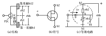
As can be seen from Figure 1, the resistance between the two bases b1 and b2 is called the base resistance:
rbb=rb1+rb2
Where: rb1----the resistance between the first base and the emitter junction, its value changes with the emitter current ie, rb2 is the resistance between the second base and the emitter junction, its value has nothing to do with ie; the emitter junction is a PN junction, equivalent to a diode.
If a positive voltage Vbb is applied between the two-sided three-pole bases b2 and b1, the voltage at point A is:
VA=[rb1/(rb1+rb2)]vbb=(rb1/rbb)vbb=ηVbb
Where: η----called the voltage divider ratio, its value is generally between 0.3-0.85. If the emitter voltage VE gradually increases from zero, the volt-ampere characteristic of the single junction transistor can be measured.
(1) When Ve��η Vbb, the emitter junction is in reverse bias, the tube is cut off, and the emitter has only a small leakage current ICeo.
(2) When Ve≥η Vbb+VD, VD is the forward voltage drop of the diode (about 0.7 volts), the PN junction conducts forward, Ie increases significantly, the resistance of rb1 decreases rapidly, and Ve decreases accordingly. This characteristic of voltage decreasing as current increases is called negative resistance characteristic. The critical point P at which the tube enters the negative resistance region from the cutoff region is called the peak point, and the corresponding emitter voltage and current are called peak voltage Vp and peak current Ip, respectively. Ip is the forward leakage current, which is the minimum current required to turn on the single junction transistor. Obviously, Vp=ηVbb
(3) As the emitter current ie continues to rise, Ve continues to decrease. After it drops to point V, Ve no longer decreases. This point V is called the valley point, and the corresponding emitter voltage and current are called valley voltage, Vv, and valley current Iv. (4) After passing point V, the carriers in the semiconductor between the emitter and the first base reach saturation, so when uc continues to increase, ie slowly rises. Obviously, Vv is the minimum emitter voltage to maintain the conduction of the single junction transistor. If Ve < Vv, the tube is cut off again.
II. Main parameters of single junction transistors
(1) Base resistance Rbb When the emitter is open, the resistance between the bases b1 and b2 is generally 2-10 kilo-ohms, and its value increases with temperature.
(2) Voltage divider ratio η A constant determined by the internal structure of the tube, generally 0.3-0.85.
(3) Reverse voltage between eb1 Vcb1 When b2 is open, the reverse withstand voltage between base b1 and emitter e at the rated reverse voltage Vcb2.
(4) Reverse current Ieo When b1 is open, the reverse current between eb2 at the rated reverse voltage Vcb2.
(5) Emitter saturation voltage drop Veo The voltage drop between eb1 at the maximum emitter rated current.
(6) Peak current Ip The emitter current when the emitter voltage is the peak voltage when the unijunction transistor is just turned on.