


Coupling refers to the phenomenon where there is a close coordination and mutual influence between the input and output of two or more circuit elements or circuit networks, and energy is transferred from one side to the other through this interaction. A coupling circuit is the circuit that participates in the coupling process.
A schematic diagram of a coupling circuit shows that, from a circuit perspective, it can always be divided into a driving source and a driven load. If the load capacitance is large, the driving circuit needs to charge and discharge the capacitor to complete the signal transition. When the rising edge is steep, the current is large, and the driving current will absorb a large amount of power supply current. Due to the inductance and resistance in the circuit (especially the inductance on the chip pins, which will cause bounce), this current, relative to normal conditions, is actually a kind of noise, which will affect the normal operation of the preceding stage. This is coupling.
Basic Operating Characteristics (Taking a Phototransistor as an Example)
1. High Common-Mode Rejection Ratio (CMRR): Inside the optocoupler, the coupling capacitance between the LED and the receiver is very small (less than 2pF). Therefore, the common-mode input voltage has little effect on the output current through the inter-electrode coupling capacitance, resulting in a high CMRR.
2. Output Characteristics: The output characteristics of an optocoupler refer to the relationship between the bias voltage VCE applied to the phototransistor and the output current IC under a certain emitting current IF. When IF=0, the LED does not emit light, and the collector output current of the phototransistor at this time is called the dark current, which is generally very small. When IF>0, under a certain IF, the corresponding IC is basically independent of VCE. The change between IC and IF is linear. The output characteristics of the optocoupler measured by a semiconductor transistor characteristic curve tracer are similar to those of a common transistor. The test connection is shown in Figure 2, where lines D, C, and E correspond to terminals B, C, and E, respectively, and are connected to the instrument socket.
3. The optocoupler can be used as a linear coupler. A bias current is provided to the light-emitting diode (LED), and the signal voltage is coupled to the LED through a resistor. The phototransistor receives a light signal whose bias current increases or decreases, and its output current changes linearly with the input signal voltage. The optocoupler can also operate in a switching state to transmit pulse signals. When transmitting pulse signals, there is a certain delay time between the input and output signals; the input and output delay times vary greatly depending on the optocoupler structure.
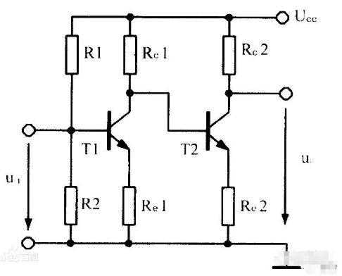
Direct Coupling Circuit Working Principle Analysis and Understanding
The direct coupling circuit was introduced in the section on two-transistor direct-coupled amplifiers. A characteristic of direct coupling circuits is that there are no coupling components between the output of the preamplifier and the input of the subsequent amplifier.
Direct coupling circuits allow both alternating current and direct current to pass through. This is a characteristic of this type of coupling circuit, so direct-coupled amplifiers can be used to amplify DC signals and have good low-frequency characteristics.
The disadvantage of direct coupling circuits is that, because DC current can also pass through, the DC circuits of the various stages of the amplifier participating in the coupling interfere with each other, which is detrimental to circuit fault repair.
4. Transformer Coupling Circuit Working Principle Analysis and Understanding
There are various specific circuit forms of transformer coupling circuits.
One type of transformer coupling circuit. Figure 3 shows a transformer coupling circuit. In this circuit, VT1 and VT2 form a two-stage amplifier; T1 is a coupling transformer, L1 is its primary winding with one tap, and L2 is its secondary winding. This coupling transformer T1 has only one set of secondary windings.
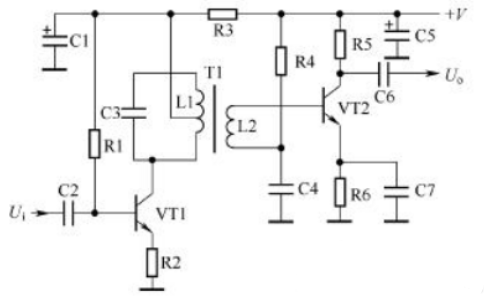
The working principle of this transformer coupling circuit is explained in the following points:
1) The collector signal current of VT1 flows through the winding below the tap L1 of the primary winding of T1. According to the transformer principle, an output signal voltage is generated across the secondary winding of T1. This output signal voltage is applied to the base circuit of VT2. The signal current loop is: upper end of secondary winding L2 → VT2 base → VT2 emitter → emitter bypass capacitor C7 → ground → capacitor C4 → lower end of secondary winding L2, forming a loop through the secondary winding L2 to complete signal transmission.
2) For DC current, since the primary and secondary windings of T1 are insulated, the DC circuit of VT1 is isolated from the DC circuit of VT2. This characteristic is the same as that of an RC coupling circuit.
3) The low-frequency characteristics of the transformer coupling circuit are poor. This is because the primary winding of the coupling transformer is the collector load of VT1. Since the inductive reactance of the winding is proportional to the frequency, the inductive reactance is small when the signal frequency is low, the collector load resistance of VT1 is small, and the voltage amplification factor is small (the voltage amplification factor of the amplifier is small when the collector load resistance is small). Obviously, the low-frequency characteristics of the transformer coupling circuit are poor. In addition, when the signal frequency is high enough, due to various high-frequency energy losses in the coupling transformer T1, the high-frequency signal is lost, so the high-frequency characteristics of this coupling circuit are also poor. The fault analysis of this transformer coupling circuit mainly explains the following points:
(1) When the tap L1 of the primary winding of the coupling transformer T1 is open, there is no DC working voltage at the collector of VT1. At this time, VT1 has no output signal, and VT2 also has no signal output, but the DC working state of VT2 remains unchanged (meaning that the DC working voltage and current of the collector, base, and emitter of VT2 remain unchanged).
(2) When the secondary winding L2 of the coupling transformer T1 is open-circuited, it does not affect the normal operation of VT1, but VT2 has no base voltage. Therefore, VT2 is cut off and has no AC signal output.
(3) When capacitor C4 is severely leaking or broken down, the DC bias voltage at the base of VT2 is low or nonexistent, VT2 is cut off, and VT2 has no AC signal output. When C4 is open-circuited, it has no adverse effect on the DC circuit of VT2, but the lower end of the secondary winding L2 of T1 has no AC ground. It can only be AC grounded through resistor R4 and capacitor C5. This is equivalent to connecting resistor R4 in series in the AC circuit of the VT2 base, significantly attenuating the AC signal input to the VT2 base, and greatly reducing the output signal of VT2.

 BR 17265
  VN 8618
  US 7107
  IQ 3858
  MY 3806
  AR 2800
  CN 2599
  BD 2159
